Triggering read and write cycles of DDR3 memories

When analyzing the signal integrity performance of DDR interfaces, separating read and write cycles has been a challenging task. Comprehensive trigger capabilities are required – especially when attempting to recreate the eye diagram in realtime.

Random overlay of DDR read and write cycles
Open Lightbox

Your task

The signal quality of the DDR interface is crucial for reliable operation of the memory system. Data eye analysis is a common method for evaluating signal integrity. The DDR architecture uses half-duplex operation, where read and write cycles happen on the same signal trace at different time intervals. To differentiate between a read and write cycle for the eye analysis, engineers look into the phase alignment of data (DQ) and strobe (DQS) signals. Using dedicated triggering to separate the read/write cycles is challenging, but it allows evaluation of the data eye over a long period in realtime.

Read and write cycles

T&M solution

The R&S®RTP high-performance oscilloscopes feature advanced trigger capabilities. The A-B sequence of the unique digital trigger system allows the setup of two consecutive trigger conditions with precise time delay and a resolution down to 1 ps. A trigger condition can be combined with logic qualifiers for other channels. Additionally, the R&S®RTP-K19 zone trigger option can simplify the setup by allowing users to define zones that qualify trigger conditions visually.

Read and write cycles

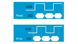
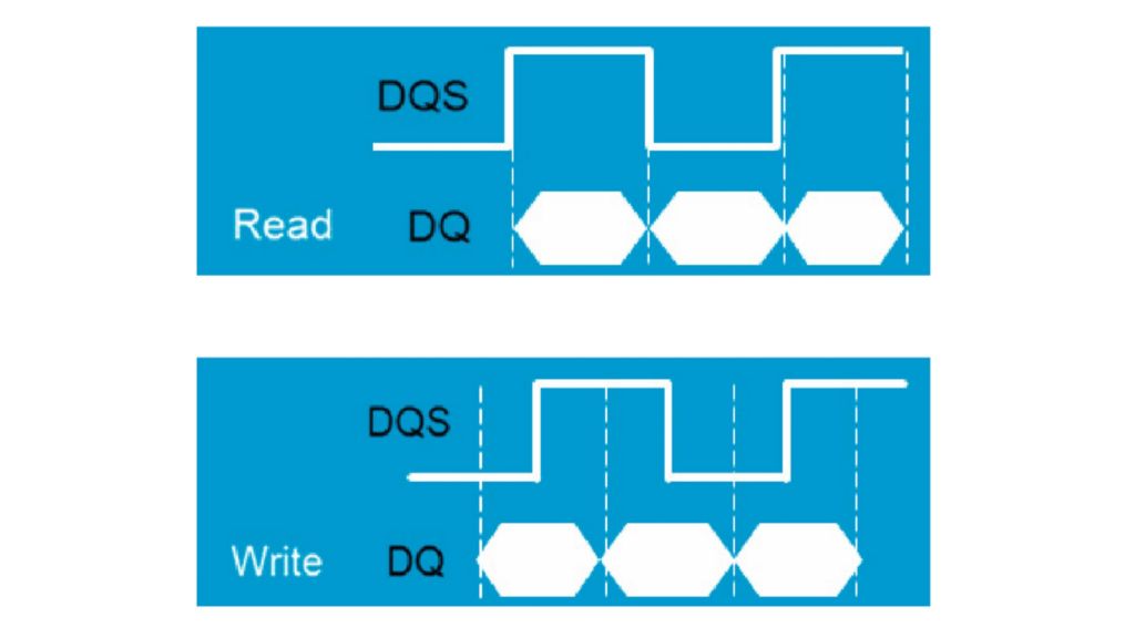
Read and write cycles of DDR memory interfaces are not phase aligned. The architecture requires a memory controller to provide differential strobe signals (DQS) to latch the data (DQ) when they are stable high or low. During the read cycle, DQS and DQ are sent in-phase from DRAM to the memory controller, but there is a 0.5 unit interval (UI) offset for the write cycle.

Setting up A-B trigger with delay
Open Lightbox

Setting up A-B trigger with delay

Leveraging the phase relationship in the write cycle, the Atrigger event can be defined as an edge trigger on the DQ signal. Then a delay and reset mechanism limits it to check for an event B edge trigger on the DQS signal. The delay to look for event B has to be within ½ UI.

Another choice for event A is a window trigger to detect the first DQ bit after returning from a tri-state sequence (window width > 1 UI).

Trigger on DQS preamble

For DDR3, the DQS preamble bit is positive on write cycles and negative on read cycles. DRAM controllers typically have a slightly different preamble bit width compared to the data bit width. This can be used as a differentiator for triggering. Simply define the width trigger on pulses longer than 1 UI or use a range from 1 UI to 1.5 UI. Since there are different preamble implementations, it is recommended to first observe the preamble timing characteristic of the device.

Trigger on DQS preamble
Open Lightbox

Trigger on DQS preamble

For DDR3, the DQS preamble bit is positive on write cycles and negative on read cycles. DRAM controllers typically have a slightly different preamble bit width compared to the data bit width. This can be used as a differentiator for triggering. Simply define the width trigger on pulses longer than 1 UI or use a range from 1 UI to 1.5 UI. Since there are different preamble implementations, it is recommended to first observe the preamble timing characteristic of the device.

Zone trigger

The R&S®RTP offers an optional zone trigger, which is useful for qualifying valid read and write cycles based on distinctive waveform shapes. Zones can be freely defined directly on the screen to distinguish if signals should or should not pass through them. This is especially useful when the waveform characteristic falls out of the trigger definition.

For write cycles, DQS is out of phase with DQ. A zone can be defined to ensure that the DQ signal does not violate the same edge as DQS.

Normally, the signal integrity of the DDR memory is measured on the DRAM side. This means that the write signal has a lower voltage amplitude than the read signal. Therefore, zone areas can disqualify read cycles based on signal strength (voltage level).

Summary

Reliably separating read and write cycles is crucial for evaluating the signal integrity of DDR memory interfaces. The digital trigger of the R&S®RTP high-performance oscilloscope ensures a precise sequential trigger mechanism. This, combined with the zone trigger, offers versatile and flexible triggering capabilities for DDR memory interface measurements.

Related solutions