Verify high frequency signal integrity on printed circuit boards

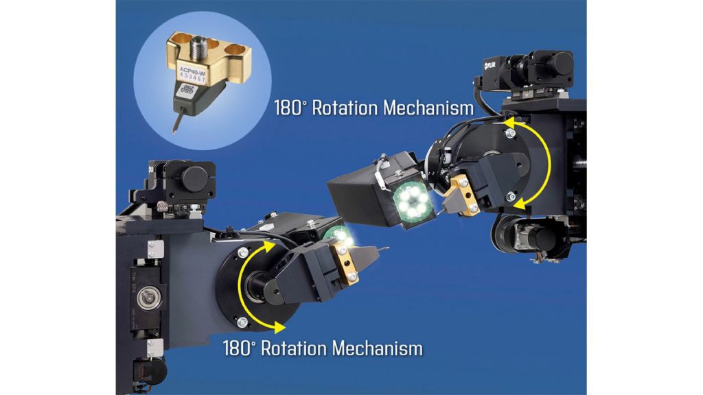
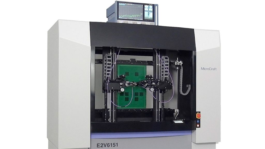
Over the past few years, electronics developers have developed a variety of approaches to avoid interference on high-speed signals on printed circuit boards. However, with increasing complexity and frequency, PCBs set new limits, supporting frequencies of 40 GHz and higher. Driven by the fast growing 5G market, today’s digital systems operate in these high frequency ranges that come with completely new challenges. With slope steepness’s of just a few picoseconds, any discontinuity in the impedance and impairment of the inductance or capacitance on the PCB or back drill defects on the PCB can have a massive impact on the signal quality. The industry recognizes that there is a growing need for functional high-speed testing of PCBs. The MicroCraft® E2V6151 series combined with an R&S®ZNB vector signal analyzer delivers a fully automated solution.

Your task

As design engineer, you want to ensure that your PCB for a 5G or data center application achieves the required signal quality with signal frequencies of 40 GHz and higher. You also want to check the success of controlled depth drilling (CDD), also known as back drilling, which is a technique used to remove the unused portion, or stub, of a copper barrel from a through hole in a printed circuit board. Comprehensive test and measurement solutions include high-end lab equipment and cost-efficient production solutions.

Verify-high-frequency_ac_en_3608-3961-92_01.jpg
Source: MicroCraft
Open Lightbox

MicroCraft solution

The MicroCraft® E2V6151 is an automated measurement system for PCBs covering a frequency range up to 40 GHz. It supports two measurement concepts: measurement of test coupons and measurement of the PCB’s high-speed signal lines. The measurement parameters are return loss, insertion loss and impedance of actual traces as well as the S-parameters of test coupons. The high frequency probe unit is equipped with a 180° rotation mechanism that allows close proximity between probes and enables testing of various pad arrangements. High frequency probes from various vendors such as the ACP series from FormFactor are supported. The probes are calibrated at the probe tip interface using corresponding calibration substrates.

Verify-high-frequency_ac_en_3608-3961-92_02.jpg
Source: MicroCraft
Open Lightbox

The PCB position is automatically recognized by the alignment camera to accurately contact with the PCB for measurements. It is equipped with a second camera to visually confirm the contact. A pressure sensor determines the contact of the probe on the board and prevents the probe from being damaged by excessively pushing it onto the board

Rohde & Schwarz solution

Particularly at higher data rates, vector network analyzers (VNA) are increasingly replacing traditional time domain reflectometry (TDR) setups for testing passive components such as connectors, cables and PCBs. Users benefit from the higher accuracy, speed and ESD robustness of the VNA as well as measurement depths for signal integrity tests, making the VNA the instrument of choice in this field

R&S®ZNB vector network analyzer
Open Lightbox

More than 60 years of experience in the field of vector network analysis pays off: Rohde & Schwarz sets new benchmarks with its R&S®ZNB vector network analyzer family. These analyzers combine high measurement accuracy with exceptional speed – better than 5 µs per point. They feature excellent temperature and long-term stability, which ensures reliable measurements over several days without having to recalibrate the units. Combined with a wide dynamic range of up to 140 dB (at 10 Hz IF bandwidth), they are the perfect measurement tool for verifying the signal integrity of high frequency PCBs up to 40 GHz

Enhanced deembedding and embedding solutions for in-fixture testing are supported in cooperation with partner companies. Their industry acknowledged software solutions are integrated into the VNA user interface. The R&S®ZNB measures the signal integrity on the PCB, taking the needed test fixtures and probes into consideration – a complete solution in a compact format.

Related solutions