System Level Verification and Debug of DDR3/4 Memory Designs
This application note provides an introduction to the DDR memory technology and explains common challenges, related to the specific nature of DDR data, command / address and control buses and describes the typical measurements to verify and debug DDR system designs.
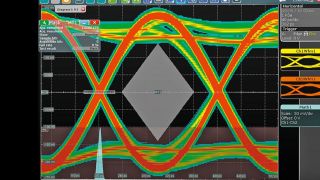
The paper explains the recommended test points and the connection of oscilloscope probes as well as the compensation of effects from DDR interposers via deembedding. The document describes efficient Signal Integrity verification with eye diagram measurements, advanced triggering and TDR/TDT functionality. Given the high number of signal lines and the dynamic bus termination, SSN (simultaneous switching noise) has a significant effect in DDR memory designs and Signal Integrity as well as Power Integrity is highly pattern dependent. We introduce techniques to achieve high acquisition rates and help to efficiently detect worst case scenarios, affecting the performance of the overall memory design. The document also includes a close look on Power Integrity.
Providing best practice examples in the design verification and debugging process, the document addresses all system designers and test engineers, working on DDR memory designs.


