Conducted emissions in DC-DC converters – simulation versus measurement

Simulation can be a big time-saver when designing EMI filters for DC/DC converters. Power supply control chip vendors offer various filter design tools that provide reasonable design choices for filter simulation before any hardware prototype is available. However, simulated results can differ significantly for different tools if simulated models are not accurate or do not cover all the relevant components. Performing a hardware measurement to evaluate the effectiveness of a simulated EMI filter is therefore indispensable.

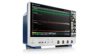
R&S®RTO6 oscilloscope

Your task

Measurements cannot be performed until the first hardware prototype is available. Power supply control chip vendors therefore offer various EMI filter design tools to provide designers with a means to gain results before any hardware is available. However, in practice, a simulated model always differs from the real hardware implementation. Designers therefore need to perform measurements on the hardware to verify the effectiveness of the simulated design. This requires the right measurement tools.

In the last few decades, the number of free power supply simulation tools from different chip vendors available on the web has drastically increased. This ongoing trend gives power supply designers the opportunity to gain deeper insight into their design concepts before the first prototype is available to perform any kind of measurements. This approach ensures that designers gain a thorough understanding of different design aspects at an early stage of development. This gives them greater confidence in their design decisions, which is likely to lead to a more reliable design. In addition, the simulated approach can help shorten the development cycle.

Power loss calculation, control loop simulation and load transient simulation are only a few functionalities that power supply simulation tools provide. The free LTpowerCAD® II Design Tool from Analog Devices is one of the most commonly used design tools on the market. Beside the above-mentioned functionalities, this tool can simulate conducted emissions in power supply designs. It provides capabilities to design and optimize EMI input filters before any hardware is available. When designers use simulation tools for this purpose, it must be clear that every simulation relies mainly on the accuracy of the simulated model. Here, designers must accept a compromise between model accuracy and calculation speed to obtain fast and efficient results. Considering that simulation results cannot cover reality in all aspects due to the limited model accuracy, it is essential to have a very good understanding of the deviation of simulated from measured results. This deviation always exists, and it is therefore mandatory to validate simulated models using suitable T&M equipment as soon as the first prototype is available.

Rohde & Schwarz solution

The R&S®RTO6 oscilloscope series with powerful multichannel FFT functionality, a line impedance stabilization network (LISN) and a suitable ground reference plane provide the required accuracy to measure conducted emissions, which are then used as a reference for comparing simulated models with the hardware implementation. Furthermore, this solution is able to separate common mode from differential mode noise. This makes it possible to directly compare measured and simulated conducted emission results. This feature is crucial sincesimulation tools usually deliver only differential mode noise as a result.

Setup for separating CM/DM conducted emissions.
Open Lightbox

Measurement and device setup

The measurement setup is illustrated in the figure “Setup for separating CM/DM conducted emissions“. It consists of a dual LISN, an oscilloscope with powerful multichannel FFT capability, and a suitable ground reference plane. To measure conducted emissions and separate common mode from differential mode noise in a power supply, an LISN with two measurement ports is required. As an alternative, two identical single-port LISNs can be used. The two coaxial outputs of the LISN have to be connected to the oscilloscope using coaxial cables, and 50 Ω input impedance has to be activated on the oscilloscope to ensure proper impedance matching. On the oscilloscope, the following steps have to be executed to measure the conducted emissions spectrum:

  • Select two FFTs and configure the minimum and maximum frequency as well as the resolution bandwidth
  • For the FFTs, select the following equations: – Ch1 + Ch2 for common mode (CM) noise – (Ch2 – Ch1)/2 for differential mode (DM) noise
  • Adjust the vertical sensitivity in the time domain window such that the input channels are not overdriven when the device under test (DUT) is powered
  • Switch off the power supply to the DUT and make a reference measurement to determine the noise floor of the setup to be able to distinguish it from the noise coming from the DUT
  • Switch on the power supply and take a measurement. Verify the result against known conducted emission limits for the DUT. Take into account any additional attenuation introduced by the LISN. In the following case study, 10 dB attenuation has been assumed for the LISN for all results.

Case study of the application

A demonstration circuit (DC3042A) from Analog Devices featuring the LTC3310 DC/DC step-down converter was chosen for the measurement setup. The board is supplied with an input voltage of 5 V and provides 1.2 V output voltage. The output is loaded with a suitable resistor to obtain a constant current of 6 A. The converter is configured to operate at a switching frequency of 2 MHz. The board features a synchronous buck topology with very low EMI. This hardware was copied to a simulation file, reflecting the hardware configuration as closely as possible to appropriately simulate the circuit with the LTpowerCAD® II Design Tool. Furthermore, another simulation file was created and executed using LTspice® from Analog Devices to evaluate an alternative simulation engine giving users more freedom, e.g. to specify parasitic components.

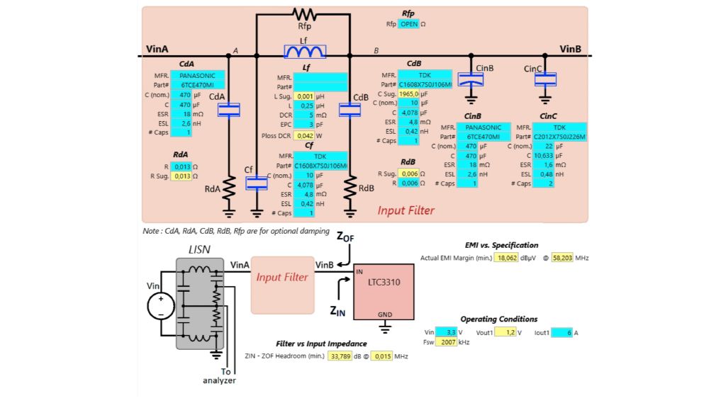
EMI input filter components and input structure.
Open Lightbox

Simulation

The schematic shows the configuration window for the input components including the EMI input filter components (“EMI input filter components and input structure“). A built-in library comprising various components from different vendors assists the user in selecting the required components. If a component is not available, the user can define its properties manually. After configuration, the user can immediately obtain the first simulation results after initiating the calculation process by pressing the update button.

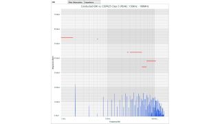
Simulated conducted EMI (LTpowerCAD® II Design Tool).
Open Lightbox

The simulated conducted emissions spectrum is now visible as shown (“Simulated conducted EMI (LTpowerCAD® II Design Tool)“). Furthermore, limit lines can be selected depending on what EMI specification the designer needs to fulfil. In addition to the EMI graph, the tool provides an attenuation and an impedance graph for the EMI filter, which are other important aspects to be observed when optimizing the filter design in terms of stability.

While the LTpowerCAD® II Design Tool helps users gain plenty of valuable information, it also has some limitations that need to be considered:

  • The tool’s EMI filter simulation part generates a given structure or circuit, but has limited capability to specify more sophisticated structures. For example, users can add only a limited number of high-frequency ceramic bypass capacitors with different values at any point in the structure
  • Parasitic components on the PCB cannot be specified

Some component types like ferrite beads are not selectable from the library and need to be configured as simple inductors.

In contrast, the LTspice® tool gives users more flexibility to define and specify almost every circuit with any types of components. Even common mode noise can be simulated if the user specifies the necessary parasitic coupling elements. While LTspice® helps users better understand the EMI behavior of their circuits, it requires greater effort and knowledge in order to specify all relevant components, and extends the simulation execution times.

Results obtained with LTpowerCAD® II Design Tool, LTspice® tool, and measurements

LTpowerCAD® II LTspice® Measurement
No filter 68 dBμV 62 dBμV 58 dBμV
EMI filter 22 dBμV 22 dBμV 32 dBμV
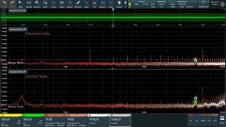
Measured conducted EMI.
Open Lightbox

Measurement

A conducted EMI measurement with the components used in the simulation was performed on the evaluation board. Common mode/differential mode separation was applied to enable a direct comparison between the measured spectrum and the simulated spectrum. The screenshot “Measured conducted EMI“ shows the relevant differential mode noise in the top window and the common mode noise in the bottom window. While the common mode spectrum plays no major role in this design, it can be valuable information in other designs, such as isolated power supply designs, in order to create an optimized EMI filter.

Deviation of simulated from measured results

The deviation of each simulated result from the measured result (see above table) was determined only at the fundamental frequency of the switching converter to reduce complexity. 2 MHz was selected as the fundamental switching frequency. Furthermore, the simulation was made with and without an EMI filter.

For the LTpowerCAD® II Design Tool, the above table shows a deviation from measured results of about 10 dB in either case, i.e. with and without an EMI filter. This gap is mainly due to the fact that no parasitic components and no high-frequency decoupling capacitors were included on the simulated PCB. Parasitic components such as series inductance and series resistance in any capacitor within a simulation circuit have shown to have a significant impact on EMI especially at higher frequencies.

The LTspice® tool provides better results since the simulated circuit reflects more closely the real evaluation board. However, for the simulation described here, relevant PCB components were still not included and unknown, and therefore a small deviation was to be expected. The LTspice® tool simulation engine tends to oscillate if reactive elements like inductors and capacitors are not damped properly. This is a necessary fine-tuning task and requires some experience on the part of the user to gain stable simulation results. On the other hand, a simulation tool such as LTspice® supports more sophisticated simulations as it allows defining electrical circuits with any parasitic components. If designers accept a greater effort to specify the most relevant parasitics as well as a longer simulation time, this tool can be a great benefit.

Summary

As results show, simulating conducted emissions may be a great help for designers to evaluate their designs in terms of conducted emissions at an early stage in development, even before the first prototype is available. However, simulated results need to be validated against measured results as soon as the hardware is ready to be measured. Only this gives designers the whole picture and understanding, and the confidence in their designs to proceed with further steps. The Rohde & Schwarz measurement solution based on the R&S®RTO6 oscilloscope featuring multichannel FFT capability and high accuracy ensures that simulated results can be validated with the first prototype.

See also

Related solutions