On-wafer characterization at sub-THz frequencies

New technologies and applications like 6G communications and sensing extend into sub-THz frequencies in the D band and beyond. New semiconductor technologies and processes need to be commercialized to support these efforts.

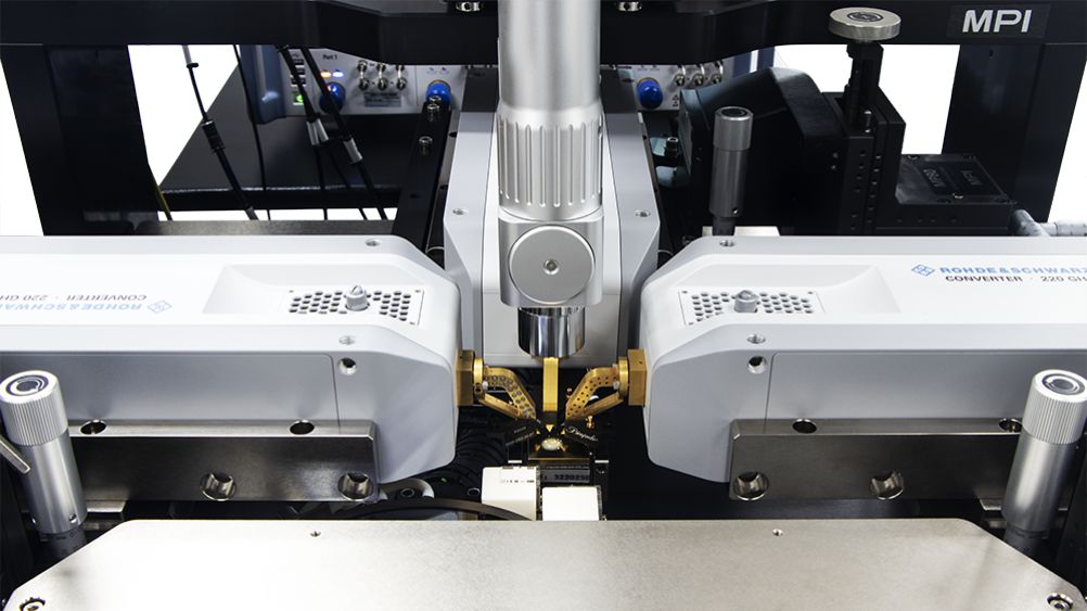
On-wafer station with integrated frequency converters allows measurement with THz frequencies
Open Lightbox

Comparing 6G requirements in terms of radio performance with respect to all the limitations that result from using higher frequencies for signal propagation, a higher throughput in terms of power and efficiency is very desirable for the millimeterwave (mmWave) or THz circuits. The performance of these RF circuits is limited by the performance of transistors and other active devices. Due to the physical limitations of transistors at these frequencies, the maximum available output power degrades drastically. For this reason, an excellent understanding of the RF behavior of semiconductor components in higher frequency applications is essential. Creating accurate models of the new semiconductor devices under different operation conditions and in a wide frequency range becomes crucial in driving applications.

Wafer-level measurement systems offered by our partner MPI Corporation with RF characteristics testing by means of a vector network analyzer are the first choice when the widest possible dynamic range of mmWave device characterization is required. Adding load-pull completes the characterization of new semiconductor components.

Your task

New communications standards and technologies use constantly higher frequency ranges to find available open spectra in the RF domain. Subsequent generations of radar sensors or future wireless systems such as 6G are foreseen to go above and beyond 100 GHz, which is also called the sub-THz range. As these bands are new to commercial applications, new semiconductor technologies need to be developed to enable cost-efficient and massproducible semiconductors. Either existing or completely new semiconductor technologies are being researched and optimized for the different applications in the high frequency ranges. Today, we already have semiconductor technologies available that can access these frequency ranges, but cost and mass availability is still an issue that needs to be addressed.
Researchers and engineers are investigating the RF capabilities of semiconductor technologies in the sub-THz region. Proven and stable methods for this purpose are available today. They are carried out directly on wafer level using appropriate wafer prober systems. S-parameters are widely used to characterize components. For a complete characterization of active components, the impedance presented to the device needs to be controlled and set by means of load-pull methods.

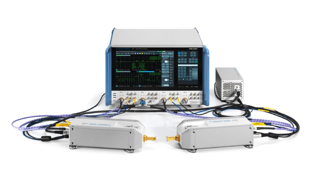
The R&S®ZNA vector network analyzer with the R&S®ZC330 millimeterwave converter for the frequency range from 220 GHz to 330 GHz.
Open Lightbox

Rohde & Schwarz cooperates with MPI Corporation and Focus Microwaves to offer a complete sub-THz and THz on-wafer load-pull system

In order to provide a full turnkey solution, Rohde & Schwarz is cooperating with the industry leaders MPI Corporation and Focus Microwaves. Each company provides its core know-how:

  • Rohde & Schwarz provides the R&S®ZNA vector network analyzer
  • Focus Microwaves provides the load-pull tuners, system software and impedance control of the test object
  • MPI provides the advanced probe station and essential hardware integration, ensuring seamless system operation
  • MPI provides integration of the mentioned instrumentation on a dedicated probe system platform supporting automated impedance tuner (AIT) applications. The system is rounded off with RF probes, calibration substrates, the probe system operation suite SENTIO® with embedded RF calibration software QAlibria®

Vector network analyzer (VNA) as core test instrument

In the test setup, the R&S®ZNA vector network analyzer is the core instrument for conducting the RF measurements. It is able to perform standard S-parameter characterization, as well as many dedicated power amplifier (PA) or mixer measurements such as gain compression, intermodulation and group delay. The base unit R&S®ZNA covers frequencies up to 67 GHz with up to 4 ports. R&S®ZCxxx millimeterwave converters extend the frequency band up to 1.1 THz allowing 4-port applications. The R&S®ZNA fully controls the frequency converters and allows easy manual or automated usage.

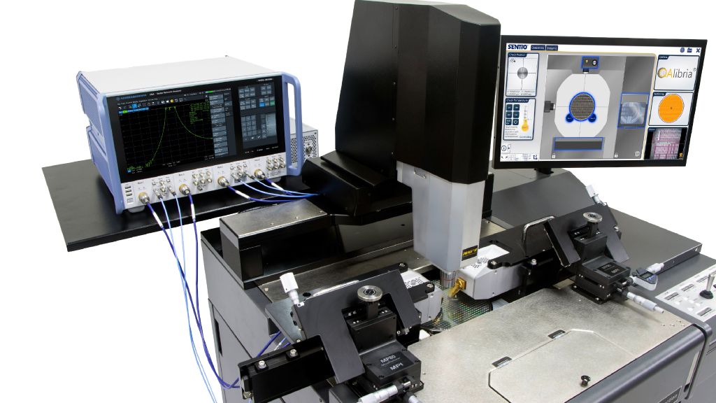
3-port on-wafer test with compact integration of Rohde & Schwarz frequency converters on MPI probe station. (©MPI Corporation)
Open Lightbox

Probe system for connection to the wafer

To meet the challenging requirements of on-wafer measurements at sub-THz frequencies, the joint solution uses the dedicated MPI Corporation probe system platform AIT. It is developed for measurements on 150 mm, 200 mm and 300 mm wafers without compromising on the instrumentation characteristics, measurement accuracy and operation simplicity. The solution covers the frequency range up to and beyond 1 THz and includes overtemperature characterization.

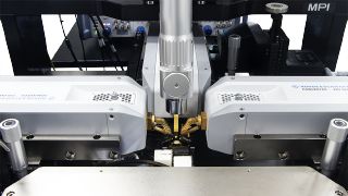
Dedicated frequency extender adaptation (FEAD) and the unique design of the probe platen enables the shortest distance between the extender port and the device under test (DUT). The fixtures position the frequency converters very close to the wafer to maximize the power into the device and guarantee an extremely wide dynamic range for measurements on its input and output. Pioneering QAlibria® calibration software and verified calibration substrates realize industry-standard and advanced calibration methods, as well as the metrological-level NIST multiline Through‑Reflect-Line (TRL) calibration by linking with the NIST StatistiCAL software package.

The manual MPI TS200-THZ probe system shares the same core principles as its automated counterpart, the MPI TS2000-IFE THZ-Selection. Both systems incorporate precision positioners and an engineered platen to ensure optimal performance during on-wafer measurements. The manual version achieves precise wafer positioning and proximity to the frequency converters, enabling accurate alignment and contact with the device under test. This design minimizes signal loss, reduces mechanical conflicts and enhances the power delivered to the device under test (DUT), making it an essential feature for sub-THz applications, including load-pull.

Similarly, the automated MPI TS2000-IFE THZ-Selection integrates advanced engineered platen and precision positioners, following the same approach as the manual version. The automated system maintains stable and controlled measurement conditions, which is critical for reliable and repeatable sub-THz measurements. Leveraging MPI’s innovative frequency extender integration design, this automated system ensures uninterrupted signal transmission, supporting RF, mmWave and THz measurements with outstanding accuracy.

Both the manual and automated versions are engineered to cater to different wafer sizes, including up to 300 mm, making them versatile solutions for a wide range of semiconductor applications. These advanced systems enable researchers and engineers to explore semiconductor technologies in the high-frequency domain, offering excellent accuracy and repeatability in on-wafer characterization.

The support of 3-port measurements, extending into the THz range is another unique capability of the MPI systems. This allows broadband subharmonic mixer testing by concurrently coupling millimeterwave and local oscillator (LO) ports.

Effect of loss on tuning range: Conventional tuner structure versus Focus Delta tuner with direct RF probe connection
Open Lightbox

Load-pull and impedance transformation

For a complete device characterization, load and source pulling is required. It allows the semiconductor device under test to be subjected to defined impedances and the DUT to be characterized across varying source and load matchings. Device modeling is one important application for load-pull. Finding the maximum efficiency behavior of an active device such as a power amplifier is another application for load-pull. The behavior of the active component with regard to maximum output power or power added efficiency is highly dependent on the applied impedances. Last but not least, the test instrumentation is typically designed for a 50 Ω environment. Active components on wafer level are a long way from this value. Impedance matching is often applied using impedance tuners for testing on wafer level.

To form a complete solution, Rohde & Schwarz partners with Focus Microwaves using their Delta tuners. The new Delta series of electro-mechanical tuners from Focus Microwaves are designed specifically for high-frequency on-wafer measurements. The low profile of the tuner means that it can be placed within the wafer perimeter, allowing direct connection between the probe tip and the tuner and thereby eliminating all possible insertion loss between the DUT and the tuner. This revolutionary new tuner design enables the engineer to achieve an optimum tuning range, with a tuner whose footprint and weight has been dramatically reduced. Focus Microwaves offers a wide range of Delta impedance harmonic tuners covering frequencies from 1.8 GHz to 110 GHz.

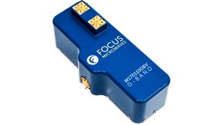
Leveraging the technology of the Delta tuners and combining it with the micro-metric accuracy and repeatability of the small footprint tuners, Focus developed a new family of waveguide tuners designed for frequencies greater than 110 GHz. Focus Microwaves small footprint waveguide tuners and state-of-the-art on-wafer integration allow for direct connection to sub-THz waveguide probes, providing maximum tuning range. Using built-in reflectometers for input and output traveling waveform (a1,2, b1,2) measurements combined with R&S®ZRXxxxL receivers, the sub-THz tuners can be used for fully calibrated vector load-pull measurements. This approach also allows for easy adaptation to hybrid techniques often used to increase the tuning range of passive load-pull systems.

Focus Microwaves waveguide tuner, model W1701100BV (©Focus Microwaves)

Application

The combined base system, comprising the VNA and the probe station, enables on-wafer measurements of RF devices. MPI Corporation provides a wide range of probes, including single-ended probes capable of reaching up to 110 GHz and multi-contact probes for advanced biasing.

With the integration of RF converters and dedicated MPI waveguide probes, researchers can extend their measurements to higher frequencies, covering the entire THz spectrum. This includes exploring the highly researched D band, which is essential for 6G activities, as well as investigating frequencies up to 330 GHz, also relevant for 6G applications. This comprehensive frequency coverage allows researchers and engineers to characterize semiconductor devices accurately, paving the way for advancements in the next generation of communications technologies.

As with every VNA measurement, calibration of the system is important and is done in two steps for the complete system:

1. Calibration of the on-wafer system with just the VNA and its converters using MPI calibration solutions and the accompanying software. For details, see the MPI application note “Simplifying the Art of Terahertz Measurements” (www.mpi-corporation.com/wp-content/uploads/ASTPDF/MPI-Simplifying-the-Art-of-Terahertz-Measurements.pdf).

2. Calibration of the load-pull tuners in the system. This is accomplished using the Focus Microwaves software.
Once calibration is complete, the Focus Microwaves software acts as the system software. It controls the applied impedance using the tuners as well as the R&S®ZNA to perform the RF measurements for device characterization.
The MPI prober ensures stable test conditions in positioning. In addition, cooling of the DUT in operation is achieved by using the cold plate plus a controlled, integrated air flow within the prober station around the wafer DUT.

Summary

Advancements in communications and sensing have expanded into the THz frequency range, driving the need for optimized semiconductor materials. Through a collaborative effort, Rohde & Schwarz, MPI Corporation and Focus Microwaves provide joint solutions for sub-THz and THz on-wafer measurements. This partnership combines vector network analyzers, probe systems and impedance tuners, enabling robust and accurate characterization of semiconductor devices at THz frequencies. Together, the three industry leaders accelerate the development of innovative technologies, unlocking new possibilities in highfrequency communications and sensing.

Detailed block diagram and achievable impedance tuning range in the Smith chart

The figure shows the D band vector load-pull setup, which includes the small footprint waveguide tuners that are connected directly to the RF probe and are available with optional integrated bidirectional couplers. These integrated bidirectional couplers allow connection of the external downconverters to measure the forward and reverse traveling waves directly at the input and output of the DUT.

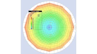
Impedance tuning range

The figure visualizes the impedance tuning range of the Focus D band WR06 tuner at 170 GHz on the tuner reference plane. It shows that a VSWR of 16:1 is easily achievable on the tuner plane. The VSWR response of this tuner is very flat across the entire band.
(©Focus Microwaves)