A 1 MHz to 50 GHz Direct Down-Conversion Phase Noise Analyzer with Cross-Correlation

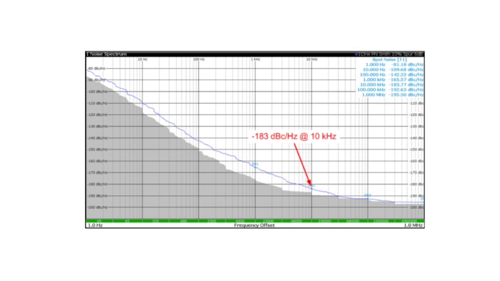
A new phase noise test instrument covers the frequency range from 1 MHz to 50 GHz with direct down-conversion analog I/Q mixers and baseband signal sampling. The traditional PLL has been replaced by a digital FM demodulator for phase detection and frequency tracking. An additional AM demodulator enables concurrent measurement of phase and amplitude noise. The instrument can measure phase noise as low as -183 dBc/Hz with a 100 MHz carrier frequency and 10 kHz offset within two minutes.

Gregor Feldhaus and Alexander Roth

Rohde & Schwarz GmbH & Co. KG Munich, Germany

gregor.feldhaus@rohde-schwarz.com, alexander.roth@rohde-schwarz.com

Introduction

Traditional phase noise analyzers use an analog phase-locked loop (PLL) to recover the phase difference between a local reference oscillator and the device under test (DUT). Setting up the loop bandwidth and phase detector characteristics correctly requires deep knowledge of the oscillator to be measured or extensive premeasurement of the DUT’s frequency drifting characteristics. The frequency response of the analog PLL must be known or calibrated to correct the final measurement result. Furthermore an analog PLL achieves only a rather poor rejection of amplitude modulation to the phase output, an effect that has recently gained attention as a cause of cross-spectrum collapse [1].

The relocation of the phase detector into the digital domain promises a much easier setup and improved measurement accuracy. The characteristics of the digital components are predefined and can be compensated with absolute precision. In [2] the RF waveforms of the local oscillator and DUT are sampled, and the phase difference of both is calculated digitally. However, the carrier frequencies are limited to the Nyquist band of the analog-to-digital converter. Additional mixers for the reference oscillator and DUT can extend this method to the microwave range [3].

The alternative approach presented in this paper employs a low phase noise local oscillator for direct down-conversion of the DUT signal. A second independent receive path enables cross-correlation to suppress uncorrelated noise in both paths. The methods described in this paper are implemented in the commercially available R&S®FSWP phase noise analyzer which is designed for phase noise and VCO measurements of continuous waveform (CW) and pulsed sources from 1 MHz up to 50 GHz [4].

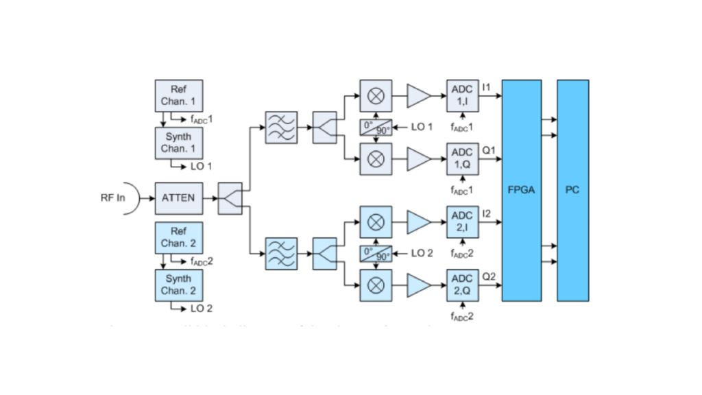
Fig. 1. Overall block diagram of the phase noise analyzer
Open Lightbox

Analog Signal Path

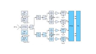
Fig. 1 shows the components of the phase noise analyzer equipped with two channels for cross-correlation measurements.

The RF signal at the input connector is split into two separate paths behind the adjustable attenuator. Each path contains an analog in-phase / quadrature (I/Q) mixer to convert the RF signal into two analog low frequency signals with 90° phase shift. The local oscillators (LO) of channel 1 and channel 2 are derived from two different reference clocks. The reference of channel 2 is loosely coupled to the reference of channel 1 by a PLL with a bandwidth of less than 0.1 Hz. This allows true cross-correlation down to frequency offsets of 0.1 Hz.

The choice between the LO frequency and the DUT frequency depends on the frequency offsets to be measured. In general, the lower the intermediate frequency (IF) of the resulting I/Q signal, the better the noise performance of the subsequent analog-to-digital converters, i.e. choosing a zero IF appears to be advantageous. For free running oscillators, on the other hand, there will always be a deviation between the true RF frequency and the LO frequency, and this causes harmonics of the difference frequency. With this in mind, a zero IF is used only for measurements above the 1 MHz frequency offset where the harmonics of the remaining frequency deviation drop to the point where they no longer disturb the measurement. Measurements below the 1 MHz frequency offset use an IF slightly above 1 MHz, and their harmonics fall outside the measurement range.

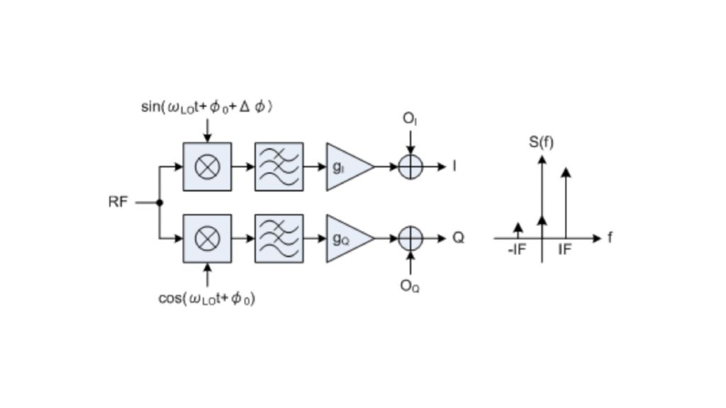
Fig. 2. Model of the I/Q mixer impairments and the resulting spectrum
Open Lightbox

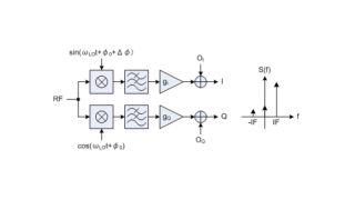
Consideration must be given to the imperfections of analog I/Q mixers as shown in Fig. 2. A deviation of the desired 90° phase shift and gain differences between the I and the Q paths cause an I/Q imbalance, which also produces AM/PM conversion. In the frequency domain, a spectral line occurs at the mirrored IF frequency. LO feedthrough adds a DC offset to the I/Q signal. Gain and phase deviations are factory-calibrated over the instrument’s frequency range, while the DC offset is calibrated prior to each measurement. Compensation of these effects is carried out in the digital signal processing path of the FPGA.

This receiver concept typically achieves an AM suppression of 40 dB compared with 15 to 30 dB of traditional analog PLLs, which reduces the likelihood of a cross-spectrum collapse due to anti-correlated AM/PM conversion.

Digital Signal Path

The choice of the analog-to-digital converter (ADC) is crucial to the performance of a fully digital phase detector. A system with an analog PLL suppresses the carrier before sampling the phase signal, i.e. it must only consider the noise dynamic range outside the loop bandwidth. With direct down conversion and carrier sampling, the ADC must cover the complete dynamic range of the input signal.

Each of the four ADCs in Fig. 1 contains four parallel channels with 16-bit resolution running at 100 MSamples/s. Each channel achieves a signal-to-noise ratio (SNR) of about 84 dB relative to full scale. The four channels are averaged, which adds an additional 6 dB to the SNR. The noise power is equally split between phase and amplitude noise. Therefore, for a signal with full scale level at the ADC input, the contribution of the white ADC noise to the phase noise without further cross-correlation gain is

LADC = (– SNR – 10∙log10(fsample) – 3) dBc/Hz. (1)

Inserting the numbers above a phase noise contribution of -173 dBc/Hz can be expected for an optimum leveled input signal. The external clock inputs of the first ADC pair and the second ADC pair are derived from different reference frequencies. The cross-correlation process further reduces the phase noise caused by ADC clock jitter.

Fig. 3. Digital signal processing for one receive path.
Open Lightbox

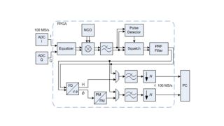
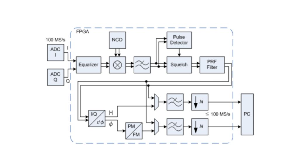
Fig. 3 shows the digital signal processing chain behind I/Q sampling.

This structure is implemented two times on an FPGA for cross-correlation measurements. The equalizer at the input of the signal chain has two functions. First, it compensates the frequency response of the filters in the analog signal path separated for the I- and the Q parts. Second, it compensates the I/Q imbalance and DC offset introduced by the analog I/Q mixer. The equalized signal can be shifted via an arbitrary frequency offset, which is set in the numerical controlled oscillator (NCO).

This is used to center the spectrum on the carrier frequency. A subsequent low-pass filter removes signal parts that fall outside the spectrum of interest.

The pulse detector, squelch and pulse repetition frequency (PRF) filter allow measurements on pulsed sources and are bypassed for standard CW measurements. This functionality is explained in detail in section IV.

Fig. 4. AM and FM demodulation of an ideal CW source.
Open Lightbox

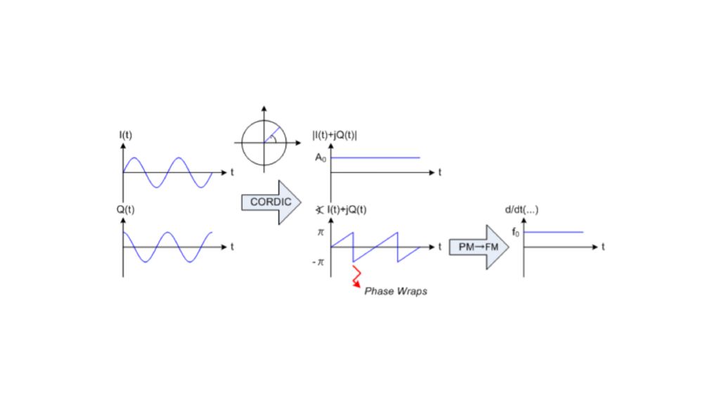
While the signal processing chain up to this point is similar to a standard digital radio concept, the following AM and FM demodulators are specific to the new approach, which allows concurrent measurement of amplitude and phase noise up to a frequency offset of 30 MHz. A CORDIC algorithm (Coordinate Rotation Digital Computer) is employed to separate the complex baseband I/Q signal into its magnitude and phase components.

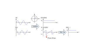
The magnitude signal is used directly to calculate the amplitude noise spectrum whereas the phase signal must be converted to a frequency signal before further processing steps (see Fig. 4).

In general, a free running oscillator will drift against the LO. The unavoidable frequency offset causes a linearly increasing phase, which wraps at the limits of ±π. The wrapping phase signal is inappropriate for further down-sampling and FFT processing. Implementing a feedback to the preceding NCO to keep the IF at zero would be an obvious solution. However, digital feedback loops tend to be problematic due to high time constants and difficult bit growth requirements. The approach presented here uses instead a phase derivation block as a reliable feed-forward structure and converts the PM signal into a non-wrapping FM signal. Slow DUT frequency drift is converted into a low- or zero frequency component of the FM signal, which does not impede the subsequent filtering and FFT processing.

Analog FM demodulators are known to be insensitive for phase noise measurements close to the carrier, as the frequency response of the demodulator decreases at a rate of 20 dB per decade toward DC. This slope must be compensated on the final measurement trace so that any white noise occurring after the demodulator, e.g. from amplifiers or a subsequent ADC, increases by 20 dB per decade. However, a digital FM demodulator shows the same characteristics toward DC. But unlike its analog counterpart, the resources of advanced FPGAs can handle the required increase of dynamic range. The digital decimation filters following the FM demodulator in the approach presented achieve a stopband attenuation of 220 dB. This covers the slope of the FM demodulator over 11 decades! The signal bit width increases accordingly to ensure that any quantization noise lies well beyond the FM demodulated phase noise.

The digital AM and FM demodulators require the carrier and the full two-sided measurement range to be present within the Nyquist bandwidth of the I/Q signal. The maximum frequency offset to be measured over the demodulator path is therefore limited to 30 MHz. For higher frequency offsets, only the sum of amplitude and phase noise is measured. In this case, the digital signal path allows the demodulator to be bypassed and transfers the I/Q data directly to the subsequent processor unit for standard spectrum calculation.

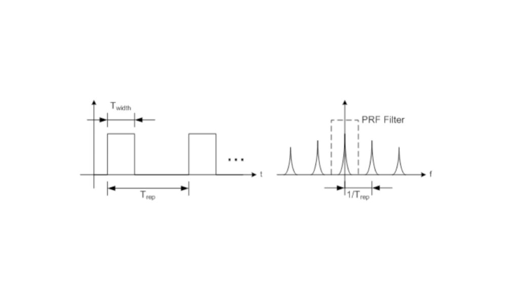
Fig. 5. Pulsed source in time and frequency domains
Open Lightbox

Pulsed Phase Noise Measurement

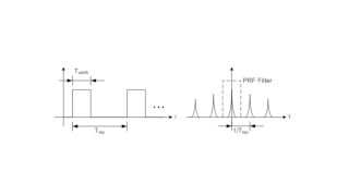
The AM and FM demodulator approach is also suitable for measuring the phase noise of pulsed sources without an additional test setup. A premeasurement determines the pulse parameters, i.e. pulse level, pulse width and pulse repetition interval. Pulsing a signal source generates a comb spectrum in the frequency domain with repetitions at the inverse pulse period as shown in Fig. 5. Meaningful phase noise measurements can be made up to half of the pulse repetition frequency. The block diagram in Fig. 3 contains a pulse repetition frequency (PRF) filter to cut off all repetition spectra except the main lobe. The output signal of the filter equals a CW signal and can be processed likewise by the AM and FM demodulator.

Before the PRF filter, an optional pulse detector and squelch block set all noise during pulse pauses to zero. This offers a remarkable advantage over analog pulse repetition filters, which add the noise power of the pulse pauses to their output signal. The difference between main lobe carrier power when pulsed and not pulsed is often referred to as the pulse desensitization factor

Pulse desensitization = 20 ∙ log10 (Twidth / Trep) dB. (2)

In the absence of countermeasures, the SNR behind the PRF filter decreases by this factor and moves the phase noise measurement closer to the instrument’s noise floor. On the other hand, setting the pulse pauses to zero reduces the noise power by

Noise reduction = 10 ∙ log10 (Twidth / Trep) dB. (3)

If both effects are combined, the sensitivity of the pulse measurement approach presented here decreases by 10 ∙ log10 (Twidth / Trep), which is only half of the complete pulse desensitization factor from (2).

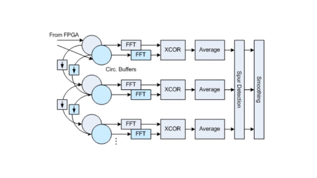
Fig. 6. FFT and Cross-Correlation.
Open Lightbox

Cross-correlation

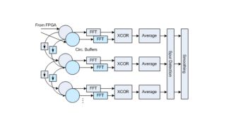
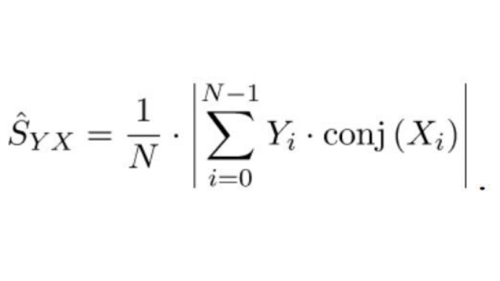
The cross-correlation and the result trace calculation is done on a standard PC processor connected to the FPGA via PCI Express. The frequency range is logarithmically divided into segments covering approximately half a decade, e.g. from 1 Hz to 3 Hz, 3 Hz to 10 Hz, and so on. Fig. 6 shows the various processing steps. The AM and FM signals from the FPGA are fed into circular buffers. The signals are continuously decimated further down to allow parallel processing of several frequency segments with different resolution bandwidths. Each segment is converted to the frequency domain via FFT. Complex conjugate multiplication of the FFT results and the following averaging block is used for the actual cross-correlation between the two independent signal paths. The estimated power density spectrum for N correlations between the FFT of the first channel X and the FFT of the second channel Y can be expressed as

conversion-phase-noise-analyzer-cross-correlation_ac_06b.jpg

Cross-correlation reduces the phase noise contribution of uncorrelated noise signals, i.e. the instrument noise arising behind the RF input splitter, by 5∙log10(N) dB, where N is the number of correlations. As long as the uncorrelated instrument noise outweighs the correlated DUT noise, the result of (4) will drop accordingly. If the correlated noise from the DUT starts to dominate over the averaged uncorrelated noise, the result of (4) settles to the true measurement result.

The instrument can stop the measurement automatically if a certain distance is achieved between the settled result of (4) and the theoretical maximum drop for uncorrelated input signals. This eliminates unnecessary measurement time for cross-correlations that do not further improve the final result.

Fig. 7. Typical noise floor with a measurement time of 10 seconds and 10 % measurement bandwidth.
Open Lightbox

Instrument Performance

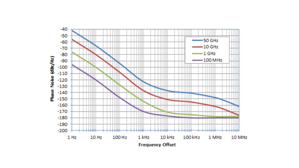
The performance of a cross-correlation phase noise analyzer is defined by its inherent instrument noise contributions and measurement speed in carrying out a certain number of cross-correlations. The internal local oscillators of the analyzer presented outperform most of the available generators and sources in respect to phase noise. Fig. 7 shows the typical system noise floor with 10 seconds of measurement time.

For frequency offsets up to 1 MHz, measurement speed is mainly determined by the physical capture time required to achieve a specific resolution bandwidth (RBW) with a given number of cross-correlations. With a Blackman-Harris window for the FFT and an overlap factor of 0.75, the capture time can be expressed by

Tcapture = 2.0 / RBW ∙ (1 + 0.25 (NXCORR-1)). (5)

Fig. 8. Two-minute phase noise measurement of a Wenzel 100 MHz-SC Golden Citrine crystal oscillator with a 19 dBm output level.
Open Lightbox

Captured data from higher frequency segments are used for concurrent calculation of subjacent segments. Combining the excellent RF performance and intelligent signal processing makes it possible to achieve unrivaled measurement speed. Fig. 8 is the result of a phase noise measurement of a top-class oscillator, which was completed in just two minutes. This oscillator was also calibrated at the United States National Institute of Standards and Technology (NIST) to verify the precision of the measurement result.

References

[1] Nelson, C.W.; Hati, A.; Howe, D.A., "A collapse of the cross-spectral function in phase noise metrology", Rev. Sci. Instrum., vol. 85, 2014

[2] Grove, J. et al., "Direct-digital phase-noise measurement", Proc. of Frequency Control Sym-posium and Exposition, 2004, pp.287-291, 23-27 Aug. 2004.

[3] Parker, S.R.; Ivanov, E.N.; Hartnett, J.G., "Extending the Frequency Range of Digital Noise Measurements to the Microwave Domain," IEEE Transactions on Microwave Theory and Techniques, vol.62, no.2, pp.368-372, Feb. 2014.

[4] Rohde & Schwarz, "R&S®FSWP Phase Noise Analyzer and VCO Tester", Product Brochure, 2015.

© 2016 IEEE. Personal use of this material is permitted. Permission from IEEE must be obtained for all other uses, in any current or future media, including reprinting/republishing this material for advertising or promotional purposes, creating new collective works, for resale or redistribution to servers or lists, or reuse of any copyrighted component of this work in other works. DOI: 10.1109/EFTF.2016.7477759

Related solutions