Realtime deembedding with the R&S®RTP
Deembedding, often a necessary and complex task, is made easier with an integrated hardware and software solution.
Deembedding, often a necessary and complex task, is made easier with an integrated hardware and software solution.
Verify the true performance of your design while reducing the impact of the signal path, probe, cables, fixtures and other accessories used to measure the signal.
Whether you are debugging a high-speed interface such as DDR or PCIe, characterizing a fast clock or analyzing a complex RF signal, you want to see the real signal and not artifacts of the test setup such as loading or reflections. The process of removing non-ideal signal path effects (attenuation, skew, loading, etc.) is called deembedding.
Removing this distortion in a realtime oscilloscope typically requires a filter with a response that will compensate for signal path effects. This filter is applied to a waveform with the expectation of signal quality improvements such as increased eye height, faster rise time or a removed reflection.
Unfortunately, there are some potential issues with this approach:

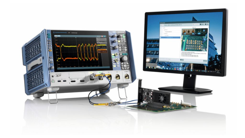
Realtime deembedding architecture
Realtime deembedding architecture
The R&S®RTP high-performance oscilloscope was designed to address these tradeoffs and offer a simple and fast deembedding solution. Multiple frequency response views of the individual circuit elements as well as the overall system responses aid in optimizing bandwidth and ensuring minimal noise amplification.
In the R&S®RTP, the deembedding filter is realized in hardware directly after the A/D converter. This realtime processing of the waveform data ensures maximum update rate even when the filter is applied. Whether you are troubleshooting a protocol error or monitoring an eye diagram, a fast, responsive measurement system ensures you do not miss any critical details.
Deembedding of cascaded signal traces
A typical signal trace structure for high-speed differential interface testing might consist of a phase-matched cable set, adapters and a test fixture. Cables, adapters and other accessories are modeled as a two-port S-parameter, while a fixture could be a two-port or four-port S-parameter. The deembedding application seamlessly manages the Sparameter cascading process while accounting for input/output loading of each block.
Superior trigger capabilities and fast signal integrity results
The final step in deembedding is to create a filter that is then applied to the signal being measured. For the R&S®RTP, the deembedding filter is available to the digital trigger and to the high-performance acquisition system. This enables the industry’s first deembedding trigger, since you can trigger on the exact corrected signal you observe. Hardware-based deembedding also speeds up critical waveform processing, for example, yielding the fastest eye diagram update rate – up to 1000 times faster than other instruments.
Improve eye margin
One of the most common questions design and test engineers ask is: What is the real performance of my design? In other words, how do you know whether the measurement reflects actual performance or whether the results are somehow influenced by test equipment loading, connector reflections, cable loss or a host of other test equipment impairments. With these known impairments, it is possible to recover design margin by using deembedding techniques. While it is advisable to always use high-quality, phase matched cables, seeing the true performance of a design is made easier with built-in compensation routines that compensate for probe loading, return/insertion loss of cables, adapters and fixtures and even the oscilloscope frontend.
")
")
USB3.0 Gen1 eye before deembedding (green waveform)
The two screenshots show a high-speed signal measured with a short (yellow waveform) and a long cable (green waveform). The long cable is deembedded and compared to the short cable response, which in this example is the ideal reference. Notice that most of the margin that was lost from the cable loss is recovered through improved eye margin.
")
")
USB3.0 Gen1 eye after deembedding (green waveform)
RF signal analysis
RF designers are continually challenged to design with more complex modulation techniques at higher frequencies and bandwidths. Each element within a signal path impacts the overall RF measurement performance. Cables, couplers, attenuators and other accessories contribute to non-ideal signal path effects such as distortion, return loss and phase error.
The frequency-dependent attenuation of a long trace is typically one of the main sources of signal-to-noise issues. Even a component as simple as a fixed attenuator can add distortion to degrade the signal more than expected. An attenuator, cable and PCB trace can easily be compensated for using deembedding techniques.
Serial triggering and decoding of deembedded signals
Finding the root cause of a design issue usually starts with reproducing the problem and isolating it with a trigger. High-speed protocol triggering and decoding become indispensable tools in correlating electrical and protocol layer activity. Ensuring the reliability of an oscilloscope protocol decoder is made possible by improving overall signal quality e.g. by deembedding.
The key to the improved trigger reliability is the increased signal amplitude and overall improved signaling characteristics that make bit and symbol detection much easier for the trigger and decode system. Traditional oscilloscope architectures include a trigger pickoff, which means the displayed deembedded signal (software corrected) does not match the raw signal seen by the trigger circuit. With the R&S®RTP, the trigger and acquisition system share the same path so what you see is what you are triggering on. This makes triggering much more reliable, even for the most complex serial buses.
As an example, a USB3.0 Gen1 signal is probed at the far end of a channel where signal loss is higher but unavoidable due to the mechanical constraints. It is still possible to decode the protocol activity, but some data may appear corrupted or out-ofsync due to hysteresis or level differences.
Serial decoding is more reliable and consistent when part or all of the channel loss compensation is applied.
USB3.0 Gen1 after deembedding
Optimizing DDR interface testing
Another signal integrity challenge made easier with deembedding is reflection removal, e.g. for verification of DDR memory systems, signal access is typically available either through direct probing of a nearby via, pin or other access point. Using a component interposer can make signal access much easier while exposing relevant signals that are routed from the ball grid array (BGA) contacts. After deembedding the interposer, this removes the fixture signal attenuation as well as the reflections caused by any impedance mismatch.
Related products