Examining receiver noise figure
RF system noise contributions define receiver capabilities and sensitivity. The noise figure measures how the critical components affect the signal.

RF system noise contributions define receiver capabilities and sensitivity. The noise figure measures how the critical components affect the signal.


Advanced communications and radar systems have ever more complex modulation schemes. The used signal bandwidth is also increasing. Both are common ways to maximize data throughput or enhance target detection resolution in radar applications. The signal-to-noise ratio (SNR) is more of a challenge in such systems. On top of everything else, the increasing carrier frequencies required to find available spectrum generate higher propagation losses and reduce signal levels at the receiver input for a given transmission distance.
In receivers, low-noise amplifiers (LNA) are typically used to compensate for losses and increase the signal level for processing. As these are active components, they always add some noise to the signal. Therefore, the noise by any components in the receiver structure must be as low as possible. The noise figure describes the amount of noise a component adds and is a key characteristic of LNAs as well as mixers and downconverters. Understanding the influence of each component is important when designing highly sensitive receivers.


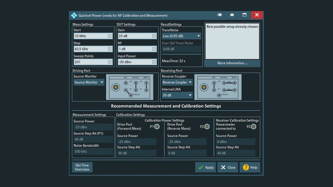
“Quickset” noise figure menu with recommendations for best measurement setup using available instrument hardware configurations and test conditions.
Various methods and different pieces of measurement equipment can determine the noise figure. But, why not just use what you have on your table?
Characterizing low-noise amplifiers (LNA), converters or transmit/receive (TRM) modules is a classic job for a vector network analyzer that examines S parameters and derived figures, such as flatness or gain compression. A vector network analyzer (VNA) not only reduces testing costs, but also allows a complete characterization using one contact, which is very important when verifying at the wafer level.
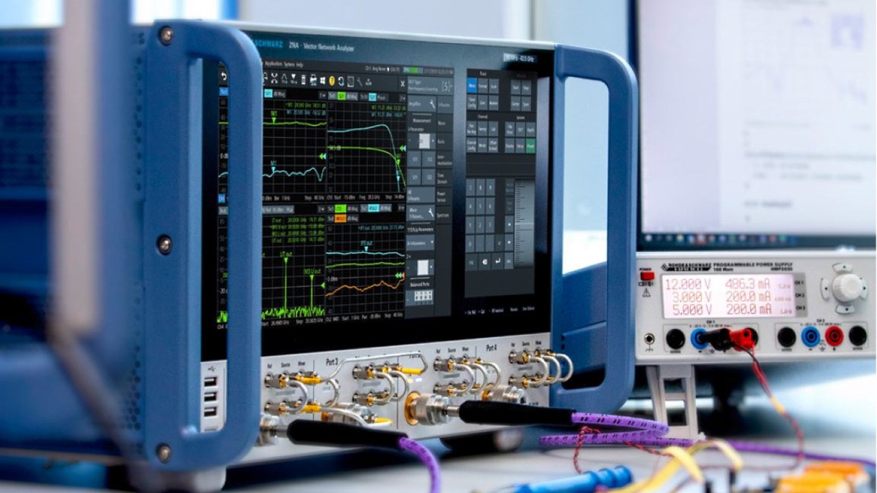
The high-end R&S®ZNA vector network analyzer offers a fully integrated noise figure test solution with guided calibration and measurements. Instead of using a noise source, the R&S®ZNA can directly measure absolute noise power based on highly accurate power level calibration. This keeps the test setup clean and minimizes the required hardware. And all characterizations can be done with a single DUT connection.
Calibration is assisted while the receiver noise figures inside the VNA are stored in the instrument using factory calibration.
As noise figure measurements are prone to errors and large uncertainties, recommendations for optimum results are very useful and help achieve best possible results at all times. Internal instrument settings are included along with recommendations for port configurations to ensure the greatest possible sensitivity and accurate noise figure measurements.
For example, when the R&S®ZNA is equipped with the source monitor option, you get direct access to the reference signal without being affected by the internal source step attenuator. This gives you a better signal-to-noise ratio and offers more accurate and faster test results. Similar “tricks” can be used at the receiver end: Using the coupler in reverse operation offers 10 dB higher sensitivity while reducing the inherent receiver noise figure.
Last but not least, the R&S®ZNA can be equipped with an internal preamplifier allowing developer to set the gain between 20 dB and 30 dB on port 2 to significantly increase sensitivity for measuring very low noise figures.
We call this interactive all-in-one noise figure setup the “Quickset” dialog. It offers all noise figure parameters and instrument configurations in a single view. You can easily get the best noise figure results and find the optimum setup with the R&S®ZNA vector network analyzer.
See also: The Cold Source Technique for Noise Figure Measurements