Verifying the true jitter performance of clocks in high-speed digital designs

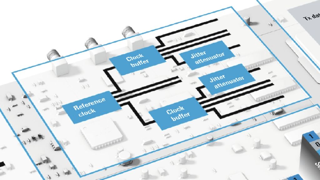
As the data rates in high-speed digital designs increase, the limits for overall system jitter become tighter. This especially applies to the various components of the clock tree, where the jitter limits for reference clocks, clock buffers and jitter attenuators are even tighter. Due to their high phase noise sensitivity, phase noise analyzers are the instruments of choice for these tests.

Clock tree
Clock tree
Open Lightbox

Your task

Measuring jitter for clocks in high-speed digital designs has become increasingly challenging. PCIe 5.0, for example, uses data rates of up to 32 gigatransfers per second (GT/s) with a corresponding jitter limit of 150 fs (RMS) for the reference clock. Data rates of 64 GT/s are introduced with a 100 fs jitter limit for the reference clock in the latest PCIe 6.0 specification. Phase noise analyzers have a superior jitter measurement floor making them ideal for measuring jitter in modern high-speed clocks. To minimize EMI effects, technologies like PCIe, USB and HDMI™ typically use spread spectrum clocking (SSC), applying a low-frequency FM to the reference clock. Since SSC puts additional stress on the clock, clock jitter also needs to be verified in SSC ON mode.

Rohde & Schwarz solution

Measuring clock jitter typically consists of:

  • Measuring the phase noise
  • Weighting the phase noise based on the corresponding system transfer function
  • Integrating the weighted phase noise in the defined jitter integration range

Measuring the phase noise

For clocks with a high slew rate, the clock jitter is mainly determined by the phase noise of the clock. Since AM noise is greatly suppressed by the high slew rate of the clock, it typically does not contribute to the overall clock jitter. For accurate clock jitter measurements, high AM suppression in the phase noise measurement is important.

Weighting the phase noise

Jitter measurements in high-speed technologies like PCIe typically need to include the system effects of the TX PLL, RX PLL and CDR transfer functions. The resulting overall system transfer function is applied to the measured phase noise trace as a weighting filter before integrating the jitter in the defined jitter integration range.

Integrating the weighted phase noise

The weighted phase noise is typically integrated up to the Nyquist frequency of the clock (half of clock rate), and in some cases even above. In that case, the phase noise also needs to be measured up to higher frequency offsets.

Jitter measurement on a PCIe reference clock (SSC ON).
Open Lightbox
PCIe clock without SSC: phase noise and weighted jitter.
Open Lightbox
PCIe clock with SSC: phase noise.
Open Lightbox

Thanks to its digital demodulator architecture, the R&S®FSWP phase noise analyzer and VCO tester measures phase noise and AM noise in parallel and provides very high AM suppression in the phase noise measurement. This architecture also makes it possible to measure reference clocks also in SSC ON mode. The instrument also features an industry-leading phase noise sensitivity, which can be further improved by adding the R&S®FSWP-B60 or R&S®FSWP-B61 option for cross-correlation. Furthermore, full spectrum and signal analyzer functionality can be added with the R&S®FSWP-B1 option to analyze coupling effects in a complex clock tree structure.

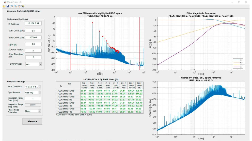
A total of 16 different system transfer functions are defined for a data rate of 32 GT/s in line with PCIe 5.0. For each of these, the weighted jitter results need to be below the limit of 150 fs. In SSC ON mode, the SSC spurs (fundamental and harmonics) up to 2 MHz need to be removed before applying weighting and jitter integration. For easy handling, an external tool can be found in the download section of this application card. This tool automates the measurement and postprocessing of the data (SSC spur removal, weighting, jitter integration and identification of the highest jitter result out of the different system transfer functions). The tool supports the R&S®FSWP (requires R&S®FSWP-B60 or R&S®FSWP-B61 option) as well as R&S®FSPN and covers PCIe versions up to PCIe 6.0.

Summary

The R&S®FSWP offers the functionality needed to test low-jitter clocks in both SSC OFF mode and SSC ON mode. It provides very high AM suppression in the phase noise measurement and excellent phase noise sensitivity for precise jitter measurements on low-jitter clocks for modern high-speed digital designs.

PCIe clock with SSC: postprocessing of phase noise trace and PCIe jitter results.
Open Lightbox